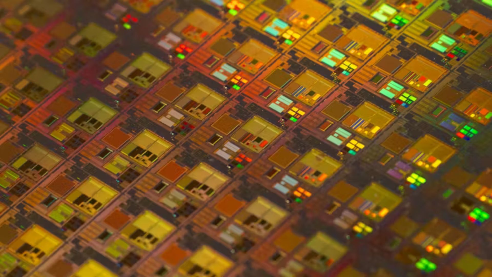
Johns Hopkins University researchers have achieved a breakthrough in microchip manufacturing that could enable circuit features so small they become invisible to the naked eye, according to findings published September 10 in Nature Chemical Engineering. The advance addresses a critical bottleneck in semiconductor fabrication by developing new metal-organic materials and a novel deposition process capable of producing circuit features smaller than 10 nanometers while maintaining economic viability for mass production (Scienmag).
The innovation targets a fundamental challenge in photolithography—the standard method for etching electrical circuits onto silicon wafers—where existing radiation-sensitive coatings fail to interact effectively with the high-energy beams required for ultra-small feature definition. This breakthrough could help semiconductor manufacturers continue meeting Moore’s Law demands while reducing costs and improving energy efficiency across applications from smartphones to quantum computing hardware.
Beyond-Extreme Ultraviolet Radiation Unlocks New Possibilities
The Johns Hopkins team developed photoresists from a novel class of metal-organic materials designed to work with “beyond extreme ultraviolet radiation” (B-EUV), which uses shorter wavelengths than current industry standards to define features below 10 nanometers. Bloomberg Distinguished Professor Michael Tsapatsis, who led the research, explained that metals like zinc absorb B-EUV light and generate electrons that trigger the chemical transformations needed to imprint circuit patterns on an organic material called imidazole.
“Companies have their roadmaps of where they want to be in 10 to 20 years and beyond,” Tsapatsis noted. “One hurdle has been finding a process for making smaller features in a production line where you irradiate materials quickly and with absolute precision to make the process economical.” The versatility of this approach proves particularly valuable because different metal atoms respond distinctly to various radiation wavelengths, with zinc emerging as optimal for B-EUV applications despite poor performance with current extreme ultraviolet systems (Hackster.io).
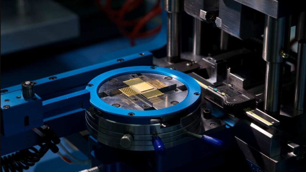
Chemical Liquid Deposition Enables Precise Control
The research team developed a methodology called chemical liquid deposition (CLD) that allows deposition of imidazole-based metal-organic resists from solution at silicon-wafer scale while controlling thickness with nanometer precision. This represents one of the first successful demonstrations of depositing these materials at industrial scale with the precision required for semiconductor manufacturing.
The international collaboration, involving institutions across three continents including Brookhaven National Laboratory and École Polytechnique Fédérale de Lausanne, explored combinations of at least 10 different metals with hundreds of organic compounds. “By playing with the two components (metal and imidazole), you can change the efficiency of absorbing the light and the chemistry of the following reactions,” Tsapatsis explained. Researchers anticipate that production lines utilizing this technology could enter commercial use within the next decade, with B-EUV radiation systems expected to reach manufacturing deployment in the same timeframe (ScienceBlog).