
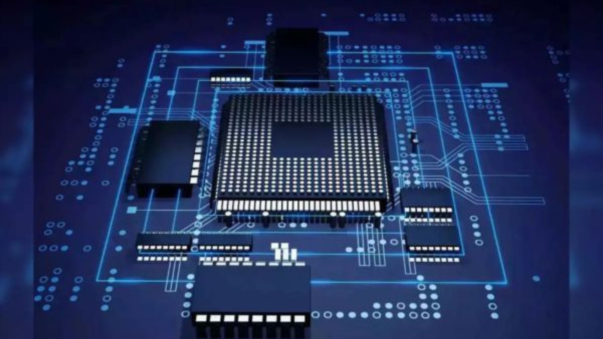
MediaTek announced Tuesday it has completed the tape-out of its first flagship system-on-chip using TSMC’s advanced 2-nanometer N2P process technology. The milestone positions MediaTek among an elite group adopting TSMC’s cutting-edge node, alongside Apple, Nvidia, and AMD, with mass production scheduled for late 2026.
Industry reports suggest the chip could be the Dimensity 9600, MediaTek’s next-generation mobile flagship processor designed to compete directly with Qualcomm’s upcoming Snapdragon platforms across smartphones, automotive electronics, and data center applications.
Technology Breakthrough Drives Performance Gains
TSMC’s N2P process marks the first commercial implementation of nanosheet transistor architecture, delivering up to 18% higher performance at equal power consumption and approximately 36% power reduction at the same speed compared to the current N3E node. Logic density increases by 1.2 times, enabling more compact designs or enhanced functionality.
“MediaTek’s innovations powered by TSMC’s 2nm technology underscores our industry leadership,” said Joe Chen, MediaTek president. Dr. Kevin Zhang, TSMC’s senior VP of business development, described N2P as “a significant step forward in the nanosheet era,” emphasizing the foundry’s commitment to energy-efficient computing.
Intensifying Competition in Advanced Semiconductors
The semiconductor industry is entering fierce competition for 2nm supremacy. Apple has reportedly secured nearly half of TSMC’s 2nm production capacity for its iPhone 18, expected in 2026, while Nvidia considers TSMC’s future A16 process for its 2028 Feynman architecture.
TSMC plans to begin 2nm mass production in H2 2025 with initial capacity of 40,000 wafers monthly, scaling to 100,000 wafers by 2026. Despite wafer costs reaching $30,000 each, demand continues exceeding expectations as companies race to leverage the performance and efficiency advantages of the most advanced manufacturing node available.